[China Instrument Network Instrument Research and Development] Lasers and optical amplifiers on the nanoscale are the core devices for future optoelectronic integration on chips, and are crucial for future information science technologies such as supercomputers and "on-chip data centers." If these nanoscale devices can be fabricated on a silicon-based substrate, it will lead the revolutionary development of on-chip optical interconnections, and thus it has become one of the focuses of the international academic community and the scientific and technological industry in the past decades.
Professor Ning Cunzheng, an expert in the Thousand Talents Program at the Department of Electronics of Tsinghua University, has long studied semiconductor luminescence physics, nanophotonics, device miniaturization, and characterization. For the first time in the world, electrolessly implanted nanolasers with a size less than half a wavelength were fabricated. For the first time, it has realized the continuous mode operation of the electric injection metal cavity nano-laser at room temperature, and is an pioneering figure in the field of nano-laser technology. Professor Ning Cunzheng's research group has been devoted to the research of physics and applications of micro-nano optoelectronic material devices, continuously breaking the limits of the miniaturization of lasers and optical amplifiers, and conducting frontier explorations for optoelectronic integration and its application in future computer chips. For more than a decade, the research group has focused on the development of nano-lasers and new optical amplifiers with high optical gain, and has recently made major breakthroughs in both areas, and on the same day of July 17th in the two sub-supplies of Nature magazine “Nature Photonics (Nature Photonics) and Nature Nanotechnology published the latest experimental results.
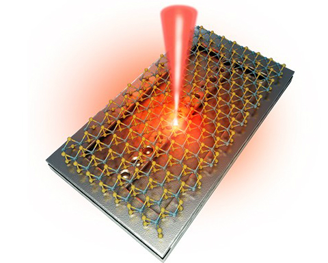
"Room-temperature continuous-wave lasing from monolayer molybdenum ditelluride integrated with a" published by Nature Research, published by Nature Science, published by the researcher Li Yongzhuo et al. (Room-temperature continuous-wave lasing from monolayer molybdenum ditelluride integrated with a Silicon nanobeam cavity), for the first time, a two-dimensional material-based nano-laser operated at room temperature in a continuous mode. This kind of two-dimensional semiconductor material with single-layer molecular thickness is highly valued in many fields. The two-dimensional material provides the thinnest optical gain material for nano-laser with its unique exciton emission mechanism. Two years ago, American scientists realized laser lasing at low temperatures in the visible light range, but room temperature operation has not been realized.
Professor Ning Cunzheng's research group has combined the experience of nano-laser research carried out over the years to use a monolayer of deuterated molybdenum with a thickness of only 0.7 nanometers as a gain material and a silicon nanoarm with a width of only 300 nanometers and a thickness of more than 200 nanometers. The cavity acts as a laser resonator. The research team found that in the above two-dimensional material, the binding energy of electrons and holes is very high, and a stable exciton state can be formed with high luminous efficiency. The silicon-based nano-arm cavity has an ultra-high optical quality factor, and the exciton radiation wavelength of the molybdenum diseloxide is barely absorbed in the silicon material. Thus, the "strong-strong" combination of two-dimensional materials and silicon-based nanoarm cavities is an important reason for raising the operating temperature of the laser to room temperature.
This research requires the fabrication of a nanometer cantilever structure with precise dimensions, and etching one-dimensional arrays of circular holes of different sizes on the cantilever. At the same time, the single-layered two-dimensional material is accurately transferred to the nano-cantilever structure. Nanotechnology presents great challenges. Professor Ning Cunzhen led young teachers Li Yongzhuo and others to overcome a series of difficulties and finally realized for the first time in the world that the two-dimensional material nano-laser operated at room temperature.
The research of nano-laser has important significance for basic research and practical application. First of all, two-dimensional materials as the thinnest optical gain materials have been demonstrated to support laser operation at low temperatures. However, whether this single-layered molecular material is sufficient to support laser operation at room temperature remains doubtful in the scientific and technological community. Room temperature operation is the premise of most practical applications of lasers. Therefore, the room temperature operation of the new laser has an index significance in the history of semiconductor laser development. In addition, due to the extremely strong Coulomb interactions in two-dimensional materials, electrons and holes always appear in the exciton state, so this laser actually interacts with a new type of exciton polariton Bose-Einstein. Cohesion is closely related and is one of the most active topics in the field of basic physics.
Assistant researcher Sun Hao and others published in the long paper "Giant optical gain in a single-crystal erbium chloride silicate nanowire" in the journal Nature Photonics. The optical net gain greater than 100 dB/cm was achieved for the first time in a single germanium compound nanowire waveguide. The research results break through the limitation of only a few dB/cm in the optical gain of traditional germanium-doped materials, laying an important foundation for realizing nano-scale high-gain optical amplifiers on silicon-based optoelectronic integrated chips.
Erbium-doped fiber amplifier is an indispensable key device in the all-optical network and information high-speed transmission system. Its advent is a revolutionary technological breakthrough in the field of optical fiber communication, making long-distance, high-speed, large-capacity optical fiber communication possible. However, in a typical erbium-doped material, the optical gain per centimeter is only a few dB due to the low concentration of cerium ions. As a result, lasers and amplifiers based on germanium-doped materials cannot be used for system integration on future photonic chips due to their large size.
In recent decades, people have been trying to find new ways to switch to high-concentration ruthenium compounds, trying to increase the optical gain by increasing the concentration of ruthenium. However, studies have found that the use of thin film epitaxial growth of germanium compounds due to poor quality of the crystal, resulting in too short a fluorescence lifetime, but also due to the high concentration of germanium will also lead to fluorescence quenching effect, there is no optical net gain reported. How to extend this successful technology model in long-distance optical communication to the field of photonic integrated chips is a major issue that needs to be solved, and it is also a research focus in recent decades.
In recent years, Professor Ning Cunzhen's research group has successfully developed a new type of single crystal germanium compound nanowire grown on a silicon substrate. In order to obtain a niobium-containing material having a high optical gain, it is generally necessary to satisfy both a high rhodium concentration and a good crystalline quality. Professor Ning Cunzhen led young teachers Sun Ye and others, after years of unremitting efforts, successfully conquered many bottleneck difficulties in single nanowire waveguide precision testing under the sub-micron scale, and finally obtained almost no defects with high quality of single crystal quality. Concentration of nanowires containing germanium. For the first time, the research team accurately measured the intrinsic absorption coefficient of the material on a single nanowire, and finally obtained an optical net gain of up to 100 dB/cm, which is much higher than the reported values ​​of other tantalum-containing materials.
This research result is of great significance for the study of basic physical properties of micro- and nano-structured materials and device applications. First, the study of the gain characteristics of germanium-containing materials lays the physical foundation for the further development of 1.5 μm photonic integrated active devices on silicon substrates working in the optical communications band; secondly, the quantum coherent lifetimes and narrow spectral lines of the germanium containing materials are combined. The features make it extremely attractive in the application of quantum information systems; in addition, the material can also be applied in fields such as solar cells, solid state lighting, and bio fluorescent tags. At the same time, this study also has reference significance for the research of nanowire structures of other rare earth elements with similar crystal quality.
Another significant aspect of the above two studies is silicon-based optoelectronics integration and future computer chips. As we all know, silicon material is the foundation of current microelectronics technology including computer chips, and is also a very promising substrate material for future photoelectric integration. However, since silicon is an extremely low-efficiency light-emitting material, it is necessary to integrate other light-emitting materials with the silicon substrate in a certain manner in the future optoelectronic integrated chips. This integration is also an unsolved problem in the integration of photovoltaics in recent decades. It is common practice to bond a light-efficient III-V compound semiconductor with silicon. In contrast, two-dimensional materials or nanowire structures do not cause any damage or performance degradation due to stress or lattice mismatch, providing a new idea for silicon-based optoelectronic integration in the future.
Both researches are the results of the cooperation between Tsinghua University and Arizona State University. The key work is completed in China. Sun Yanwei, assistant researcher in the Department of Electronics, was the first author of the article “Natural Photonics.†Other important collaborators include Dr. Yin Leijun and Dr. Liu Zhicheng of Arizona State University, and Zheng Yuze, an engineer of the Tsinghua team. Li Yongzhuo, an assistant researcher in the Department of Electronics, was the first author of "Nature Nanotechnology". PhD students Zhang Jianhang, Huang Dandan, an engineer, Sun Yan, an assistant researcher, Feng Jiabin and Wang Zhen, Ph.D. students at Tsinghua University, and Arizona State University participated in the thesis. Dr Fan Fan. Professor Ning Cunzheng is the author of two papers. The above research was supported by the independent research projects of Tsinghua University and the 1000-person plan of the Central Organization Department.
(Original Title: Ning Cunzheng Group of Tsinghua Electronics Department has made a major breakthrough in the research of silicon-based nano lasers and optical amplifiers)
Corrugated And Trapezoidal Roll Forming Machine: one layer makes corrugated panel, one layer makes IBR panel. And when the up layer is working, the down layer stops. Two layers can not work at the same time. It is used widly to roof and wall. Double metal roofing forming machine or double deck roll forming machine is a name for that.
